
Figure 4.
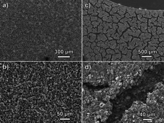
a, c) Low‐magnification and b, d) high‐magnification SEM images of sulfur electrodes with a thin coating (a, b; ≈45 μm cathode layer) and thick coating (c, d; ≈80 μm cathode layer), taken before cell assembly and cycling.
Official websites use .gov
A
.gov website belongs to an official
government organization in the United States.
Secure .gov websites use HTTPS
A lock (
) or https:// means you've safely
connected to the .gov website. Share sensitive
information only on official, secure websites.
a, c) Low‐magnification and b, d) high‐magnification SEM images of sulfur electrodes with a thin coating (a, b; ≈45 μm cathode layer) and thick coating (c, d; ≈80 μm cathode layer), taken before cell assembly and cycling.