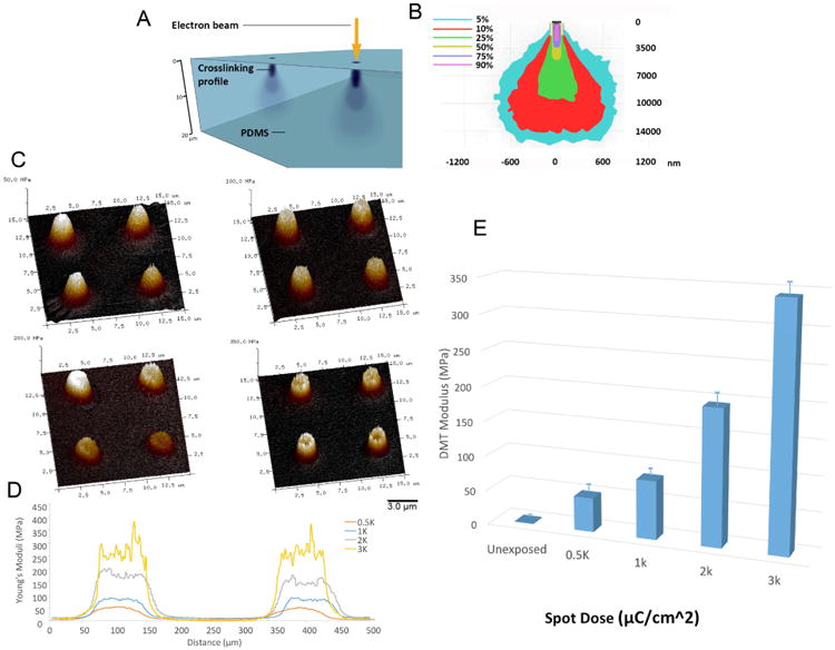
Figure 1. Electron-beam interaction with PDMS thin-films.

(A) A 120 μm layer of PDMS was deposited onto 22 mm square microscopy cover-glasses by a spin-coating process. Substrates were treated with an oxygen plasma process and coated with a final polymeric discharge layer (AquaSAVE) prior to e-beam patterning. A focused e-beam was rastered over the substrate surface to create arrays of defined surface features (spots) possessing a sub-surface rigidity gradient. (B) Monte Carlo simulations identified the electron trajectory and scatter profile in PDMS substrates. (C,D) Peak-force quantitative AFM nanomechanical mapping (PF-QNM) of 2 μm spots indicated the e-beam exposure of the PDMS film causes an increase in the elastic modulus of the polymer as a function of e-beam dose. (E) shows the function relating Young's modulus changes due to the e-beam exposure dose.
