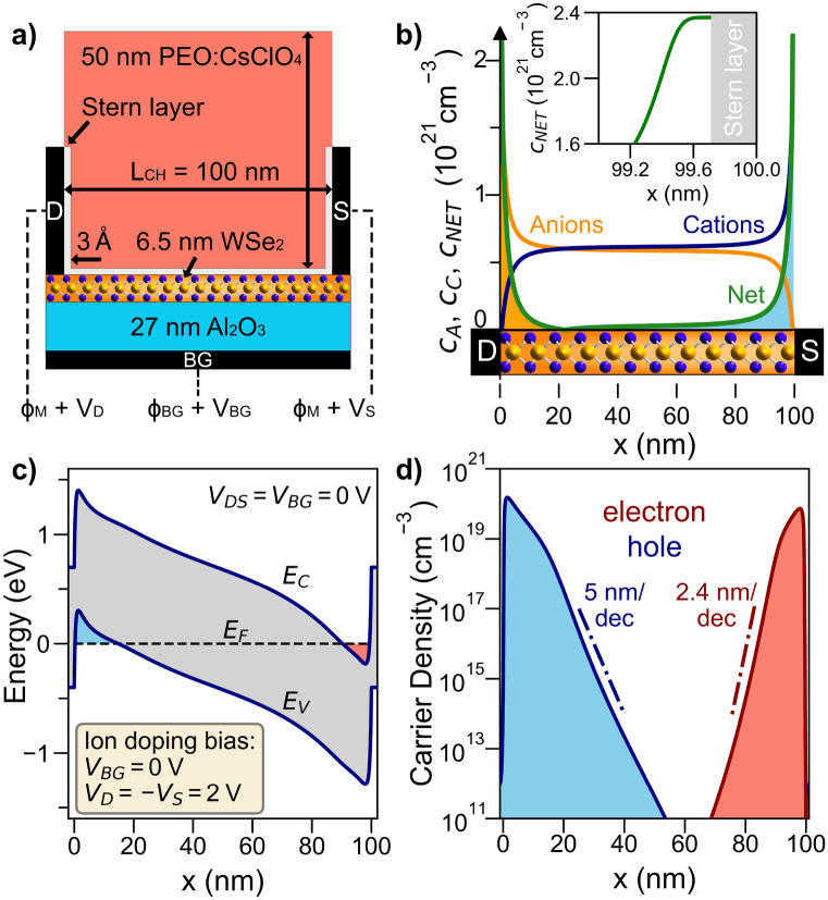
Figure 4.
COMSOL simulations of the EDL p–i–n junction in WSe2. (a) Simulated device structure, representing a scaled-version of the fabricated device consisting of a 100 nm WSe2 channel and including source, drain, and backgate metal contacts, with PEO:CsClO4 on the surface. PEO:CsClO4 is modeled as a dielectric with εPEO = 7 and a concentration of 1,000 mol/L of monovalent ions. A thin, 0.3 nm vacuum layer at the metal/semiconductor interfaces with PEO:CsClO4 represents the effect of the Helmholtz layer. (b) Computed steady-state ion profile after a bias of VD = − VS = 2 V is applied at the drain/source metal contacts. (c) Simulated band diagram along the channel length after the ion locking step at 220 K. (d) Charge density profile along the same cut showing an accumulation of image charges at the two ends of the channel, several orders of magnitude higher than that concentration in the middle of the channel.

