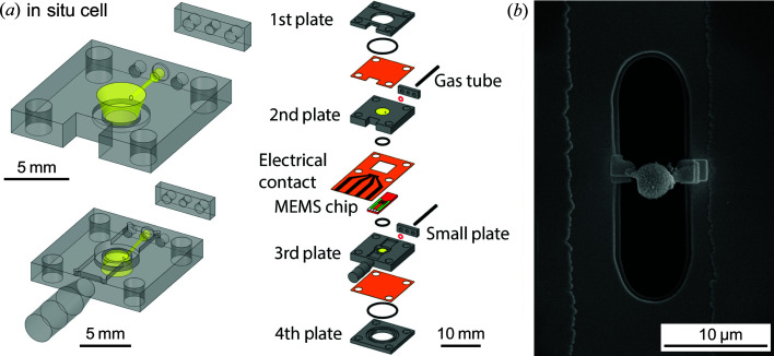
Figure 14.
(a) A schematic diagram of the sample environment for in situ ptychography with a limited tilting angle, including the MEMS chip sample holder (Fam et al., 2019 ▸). (b) A SEM image acquired during FIB–SEM showing a CoMn2O4 spinel ‘hollow-sphere’ particle of approximately 3 µm diameter attached to the viewing window of the MEMS chip.

