Figure 2.

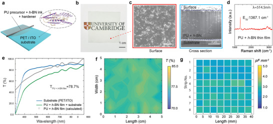
a) A schematic diagram of the K‐bar coating technique for the deposition of PU precursor+h‐BN ink. b) Photo of the printed ink layer to show the transparency and c) the corresponding SEM images of the surface morphology and the cross‐sectional view. d) Raman spectroscopy of the coated PU+h‐BN thin film showing the presence of exfoliated h‐BN flakes. e) Transmittance measurement by UV–vis spectroscopy of the printed thin film. f) Transmittance mapping across a sample area of 5 × 5 cm2 and g) capacitance mapping consists of 64 points (8×8 grids) to demonstrate optical and capacitive uniformity of the thin film.
