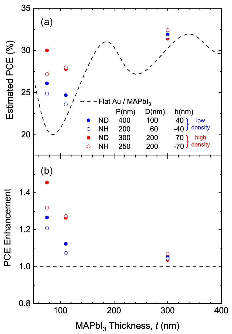
Figure 5.
(a) Power conversion efficiency (PCE) and (b) PCE enhancement estimated from experimental absorptance spectra for varying MAPbI thickness values, t = 75, 110 and 300 nm with low (blue symbols) and high (red symbols) surface density of optical scatterers in NH (open symbols) and ND arrays (solid symbols). The dashed lines represent the PCE of flat-interface structures as a function of MAPbI thickness. A strong PCE enhancement is clearly demonstrated for high-density nanostructures at t = 75 and 110 nm (red symbols).

