
Fig. 3. Inkjet printing of 2D crystals.
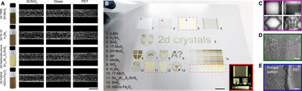
(A) Ink examples and corresponding optical micrographs of printed single lines on Si/SiO2. Scale bar, 100 μm. The inks are diluted for clarity. Brightness and contrast of the lines are enhanced to reflect the distribution of printed flakes. TMD, transition metal dichalcogenide; h-BN, hexagonal boron nitride. (B) Printed patterns on PET: (1 to 13) individual patterns and (14) gradient printing. Scale bar, 1 cm. Inset shows 3, 11, 12, and 14 with a dark background. Corresponding (C) optical micrographs of selected areas in 1, 2, 3, and 5. Scale bar, 500 μm. (D and E) SEM in 9 and 13. Scale bars, 100 μm. Photo credit: Guohua Hu, University of Cambridge and The Chinese University of Hong Kong.