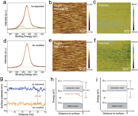
Figure 2.

Surface chemical and electrical analysis. a) XPS peak of Sb 3d5/2 obtained from the surface of as‐deposited Sb2Se3. b) AFM image of the as‐deposited Sb2Se3 surface, and c) is the corresponding KPFM image obtained by scanning the same area. d) XPS peak of Sb 3d5/2 obtained from the surface of Se‐modified Sb2Se3. e) The AFM image of the Se‐modified Sb2Se3 surface, and f) the corresponding KPFM image obtained by scanning the same area. g) Potential profiles obtained along the two lines indicated in (c) and (f). Schematic diagrams of surface band bending of h) an as‐deposited Sb2Se3 film and i) a Se‐modified Sb2Se3 film.
