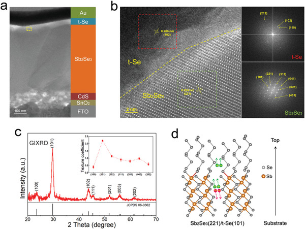
Figure 3.

Interface structure and orientation. a) Cross‐sectional TEM image of the Sb2Se3 solar cell. b) HRTEM images of Sb2Se3/t‐Se interface and the Fourier transforms of corresponding lattice fringe. c) XRD pattern of t‐Se layer on the Sb2Se3 substrate using GIXRD mode. d) Atomistic model of [101]‐oriented 1D t‐Se on the (221) plane of Sb2Se3.
