Figure 1.
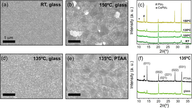
SEM top view images showing the morphology of evaporated FA0.7Cs0.3Pb(I0.9Br0.1)3 perovskite films on glass as-deposited (a) and after 30 min of annealing at 150 °C (b). (c) Room-temperature XRD patterns corresponding to evaporated perovskite films on glass following annealing at different temperatures for 30 min. Peaks corresponding to additional PbI2 and CsPbI3 phases are labeled; the other peaks correspond to the alloyed perovskite. SEM top view images displaying the morphology differences when the perovskite films are evaporated on glass (d) and PTAA (e) and annealed at an optimum temperature of 135 °C; their corresponding XRD patterns (f). The perovskite XRD peaks are assigned based on Pawley refinements (Figure S4). XRD patterns are vertically offset for clarity.

