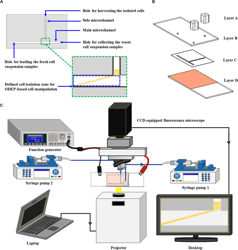
FIGURE 1.
Schematic presentation of the (A) top-view design layout and (B) the structure of an ODEP microfluidic chip (Layer A: two PDMS adapters for tubing connection; Layer B: an ITO glass; Layer C: a double-sided adhesive tape with a hollow T-shaped microchannel; Layer D: an ITO glass coated with a photoconductive layer), and the (C) the whole operating setup.

