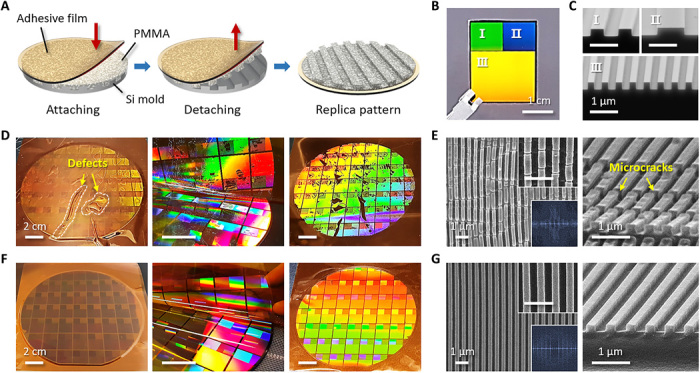
Fig. 1. Replication of nanopatterns at the 8-inch wafer.

(A) Schematic illustration of the fabrication process of the polymer replica pattern. The spin-coated poly(methyl methacrylate) (PMMA) thin film on the Si master mold, consisting of nearly 50 chips, is peeled off using an adhesive PI film. (B) One chip with three types of line/space patterns makes up a Si wafer. The linewidths of the green area (top left), blue area (top right), and yellow area (bottom) are 500 nm/500 nm, 1 μm/1 μm, and 250 nm/250 nm, respectively. (C) Tilted scanning electron microscope (SEM) images of (B). All of the line patterns have the same depth of 250 nm. (D) Photograph images after attaching (left), during the detachment process (middle), and after detaching (right) during the replication process step, all done by hand. (E) Top-view and tilt-view SEM images of (D), showing defective replica patterns with distortions and many microcracks. (F) Photographs taken after attaching (left), during detachment step (middle), and after detaching (right) during the replication process step using a roll-pressing system. (G) Top-view and tilt-view SEM images of (F), showing well-defined PMMA line/space patterns. Scale bars, 1 cm (B), 1 μm [C, E, and G; insets in (E) and (G)], and 2 cm (D and F). Photo credit: T. W. Park (KICET and Korea University).
