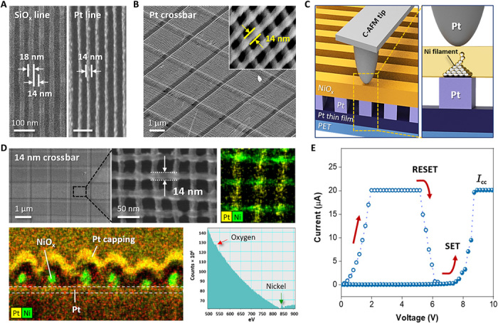
Fig. 4. High-density memristive crossbar NiOx/Pt nanoarrays via the T-nTP process on a flexible and transparent PET substrate.

(A) (Left) Self-assembled SiOx line with an 18-nm-width master template formed by the DSA of a cylinder-forming PS-b-PDMS BCP and (right) the transferred 14-nm-width Pt line pattern via the T-nTP process using the SiOx line master mold. (B) Three-dimensional hierarchical ultrahigh-resolution Pt crossbar structure produced by a repeated T-nTP process with different angles (0° and 90°). (C) Schematic illustration of the resistive memory device structure and its resistive switching mechanism through the formation of a Ni filament within NiOx nanowire. (D) High-density NiOx/Pt crossbar resistive memory device created by the T-nTP process. (Top left and top middle) Top-view SEM images, (top right) top-view transmission electron microscopy (TEM)–energy-dispersive spectrometry (EDS) elemental mapping image, (bottom left) cross-sectional TEM-EDS image, and (bottom right) an electron energy-loss spectroscopy measurement result for the NiOx line structure. (E) I-V curve of the NiOx/Pt memristive structure. Scale bars: 100 nm (A), 1 μm [(B) and top left in (D)], and 50 nm [top center in (D)].
