
Figure 5.
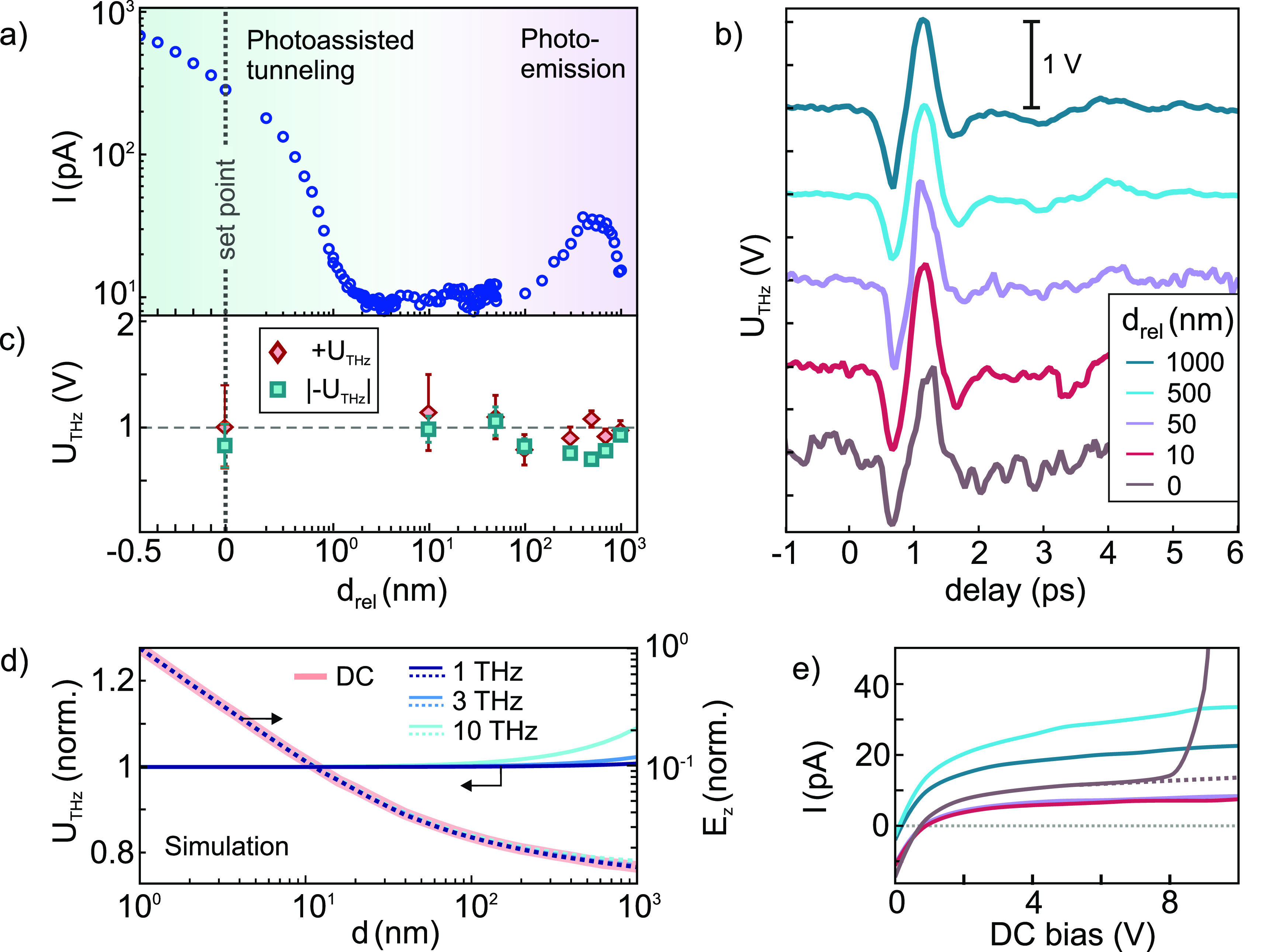
Dependence of the (a) photocurrent, (b) tip-enhanced THz waveform, and (c) peak THz voltage of the positive and negative half cycle on the tip–sample distance relative to a set point of I = 200 pA and UDC = 10 V. Nearly identical THz waveforms and constant THz voltages are observed. (d) Numerical simulation of the THz potential difference induced between tip and sample (blue solid lines, left y-axis). The THz electric field (blue dashed lines) and DC electric field (light-red solid line) in the STM junction are plotted at the right y-axis (Ez is taken 0.1 nm below the tip center; plotted values are normalized). (e) I–V curves used for THz voltage calibration (waveform sampling performed at UDC = 8 V). At drel = 0 nm, the dashed line is used for calibration, which is the photocurrent I–V without background from DC field emission, which is assumed to exponentially increase with bias.