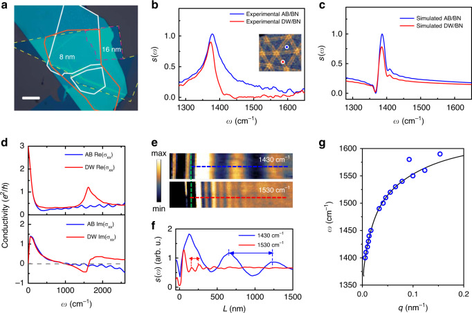
Fig. 2. Nano-FTIR spectra and phonon polariton dispersion of encapsulated TBG heterostructure.
a Optical microscope image of the twisted bilayer graphene (red solid and dash) encapsulated with 8 nm (16 nm at folded region), top h-BN (yellow solid) and 20 nm bottom h-BN. Scale bar: 10 μm. b Nano-FTIR spectra taken at AB/BA domain (blue solid line) and on the domain wall (DW) (red solid line). Inset: domain walls imaged through phonon polariton in h-BN. The blue and red dots indicate the tip locations where nano-FTIR spectra were taken at AB/BA and domain wall, respectively. Data were normalized to the signal of SiO2/Si substrate. c FDTD simulated spectra calculated for AB/BA domain (blue solid line) and along the domain wall (red solid line). d Tight-binding model calculated frequency dependence of the real part (top) and imaginary part (bottom) of the local conductivity σxx for the center of the soliton regions (red solid line), and the uniform regions (blue solid line). The soliton width is 10 nm and EF = 50 meV. e Near-field amplitude image of the h-BN/graphene/h-BN at frequency ω = 1430 cm−1 (top) and ω = 1530 cm−1 (bottom). The green dashed lines indicate the edges of the heterostructure. f Line profiles taken along blue and red dashed lines in e. Double arrows indicate λp/2. g Measured dispersion relation of the phonon polariton in the heterostructure (blue circles). Black solid line is the theoretic prediction.

