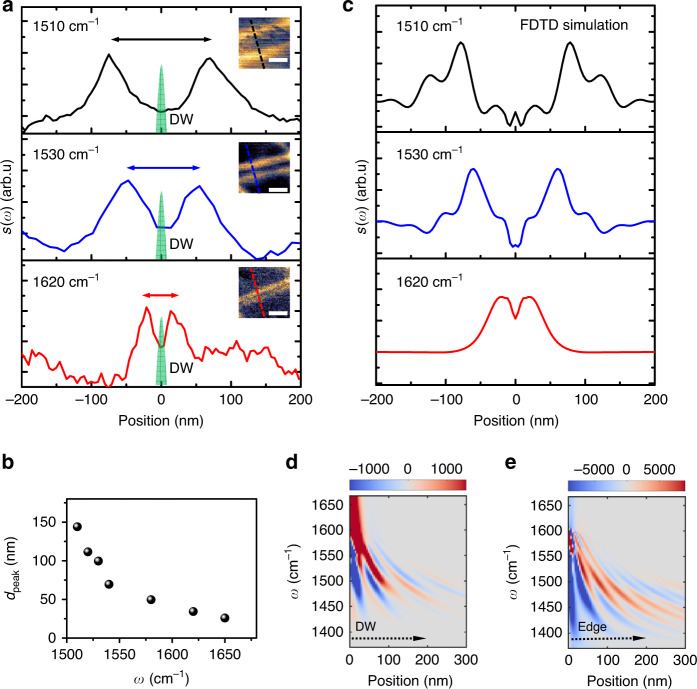
Fig. 4. Phonon polariton reflectance at the domain walls in the underlying TBG.
a Phonon polariton interference profiles across the same domain wall (DW) under excitation frequency ω = 1510 cm−1 (top panel), ω = 1530 cm−1 (middle panel) and ω = 1620 cm−1 (bottom panel). The green shaded areas label the domain wall with width of about 10 nm. The double arrows in the top (black), middle (blue), and bottom (red) indicate the distance between the two symmetric peaks dpeak. Insets: Mapping of amplitude s(ω) of the domain wall. Dash lines indicate where the profiles are taken respectively. Scale bars: 100 nm. b Distance between the two symmetric peaks dpeak (black dots) as a function of excitation frequency ω. All data points are extracted at the same domain wall. c FDTD simulations of the phonon polariton interference profiles shown in a. d, e Dispersion of the phonon polariton interference profile calculated with FDTD simulations for frequencies ω = 1380 cm−1 to ω = 1670 cm−1 while varying positions of the sampling tip with respect to the domain wall (d), and the edge of the heterostructure (e). The simulated tip scanning directions are indicated by the dashed arrows.

