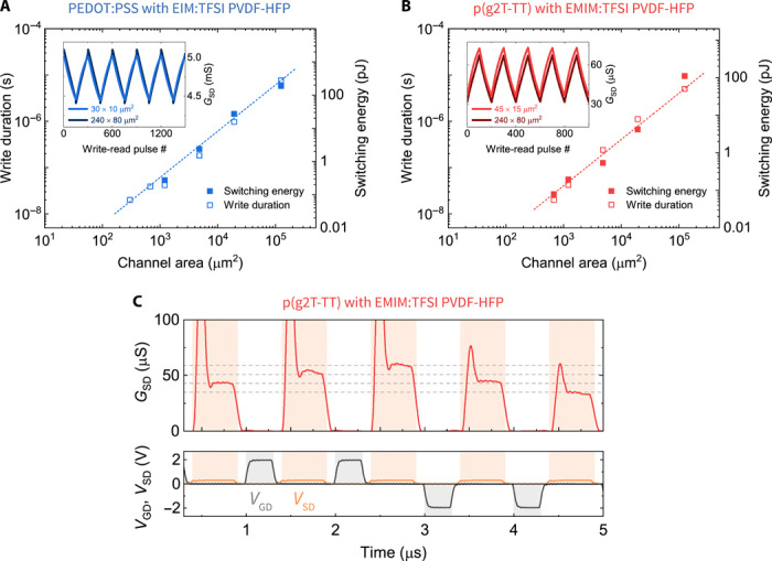
Fig. 3. Device write speed and energy scaling and operation under <1-μs write-read cycles.

Switching speed (open squares) and energy (solid squares) scaling of (A) PEDOT:PSS EIM:TFSI PVDF-HFP and (B) p(g2T-TT) EMIM:TFSI PVDF-HFP devices versus ECRAM channel area. Insets in (A) and (B) show no substantial difference in the switching characteristics of different size devices using scaled write duration. Device modeling (colored dashed lines) predicts that a 1 μm by 1 μm device will enable <20-ns switching with <10 fJ per write switching energy. (C) p(g2T-TT) EMIM:TFSI PVDF-HFP device potentiation and depression under ±2-V 200-ns write pulses (gray shaded area), followed by 100-ns write-read delay and +0.3-V 500-ns readout (orange shaded area). The horizontal dashed lines are a guide to the eye. All measurements were performed under 2 × 10⁻⁴ mbar vacuum.
