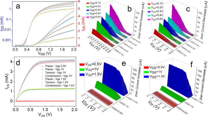
Figure 3.
I–V characteristics of the fabricated bendable transistors. (a) Transfer characteristic of MOSFET (also shown in a semi-logarithmic scale) at planar, 21 × 10–4 nominal compressive strain, and 21 × 10–4 nominal tensile strain bending conditions at different drain voltages (0.1, 0.2, 0.3, 0.4, and 0.5 V). (b) Visualization of drain current increase when the fabricated MOSFETs experience 21 × 10–4 nominal tensile strain at the same drain voltages used in (a). (c) Visualization of drain current decrease when the MOSFETs experience 21 × 10–4 nominal compressive strain at the same drain voltages used in (a). (d) Output characteristics of MOSFET at planar, 21 × 10–4 nominal compressive strain, and 21 × 10–4 nominal tensile strain bending conditions at different gate-voltages (0.5, 1, and 1.5 V). (e) Visualization of drain current increase when the MOSFETs experience 21 × 10–4 nominal tensile strain at the same gate voltages used in (d). (f) Visualization of drain current decrease when the MOSFETs experience 21 × 10–4 nominal compressive strain at the same gate voltages used in (d).

