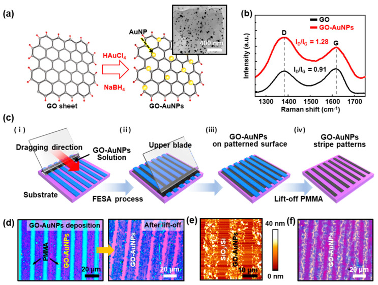
Figure 3.
(a) Schematic drawing of the synthesis of graphene oxide (GO)/AuNPs and transmission electron microscopy (TEM) image (inset); AuNPs uniformly distributed along with the basal plane in GO sheets via co-reduction process. (b) Raman spectra of pristine GO and GO/AuNPs. (c) A series of schematic illustrations for the template-assisted self-assembly of stripe patterned GO/AuNPs surface. (d) Optical micrographs of the patterned film surface of GO-AuNPs on the SiO2/Si substrate after the lift-off of the stripe patterned PMMA from C = 0.125 mg mL−1; arrows in highly magnified images show initial sacrificial PMMA patterned arrays (left) and, after the lift-off process, left behind the stripe patterned GO/AuNPs (right). (e) A typical AFM height image of stripe patterned GO/AuNPs’ surface on the SiO2/Si. (f) Optical micrographs show stripe patterns of wrinkled surface structures.

