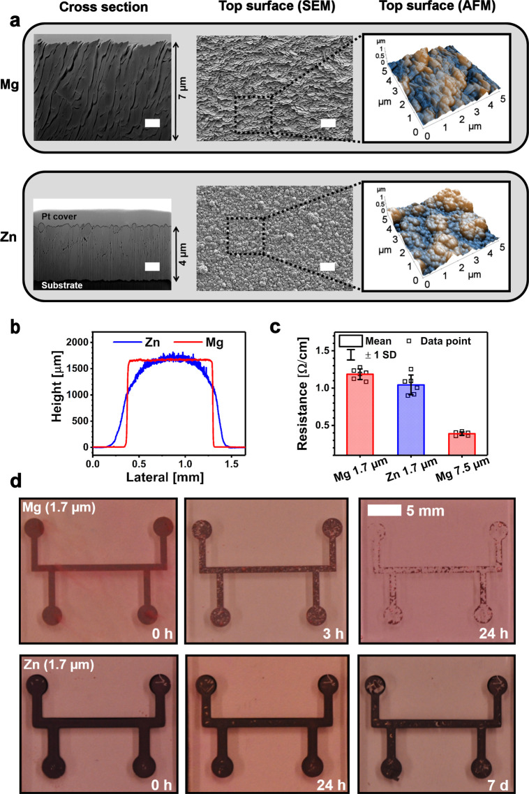
Figure 3.
(a) Structure of the evaporated Mg (7.5 μm) and sputtered Zn films (∼4 μm) illustrated by FIB-SEM, FE-SEM, and AFM techniques. White scale bars 1 μm. (b) Cross-sectional profiles of the 1.7 μm thick Mg and Zn films. (c) Electrical resistances of the ∼1 mm wide Mg and Zn films given as mean ± standard deviation (n = 6). (d) Photographs of the metal films in cell culture medium at +37 °C in 5% CO2.

