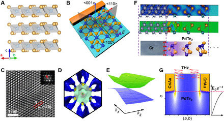
Fig. 1. Characterization and interface behavior of type II DSM PdTe2.

(A) Crystallographic structure of PdTe2. Orange and blue balls denote Te and Pd atoms, respectively. (B) Microscopic view of the metal-PdTe2 contact along with the atomic chains. The shaded area represents the mirror planes on the (001) surface. (C) HR-TEM images of PdTe2 single crystal. (D) The coexistence of hole and electron pockets in the Fermi surface along the kx-ky plane as a result of the type II Dirac cone. The hole pocket was marked by the red dotted circle, whereas the electron pocket, corresponding to the translucent aqua-like pocket, forms an apple pit–shaped pocket in the reciprocal space. (E) The projection of the Dirac cone along the kx-kz plane. The tilted Dirac cone is evident along the kz direction. (F) The charge density (top) and charge density difference (middle) near the metal (Cr/Au)–PdTe2 interface. The bottom panel represents a schematic diagram of the corresponding range of atomic structures. (G) The cross-sectional view of localized-field distribution along the c axis near the metal-PdTe2 interface under terahertz illumination.
