
Fig. 3. The anisotropic photocurrent of the PdTe2-based device at zero-bias voltage.
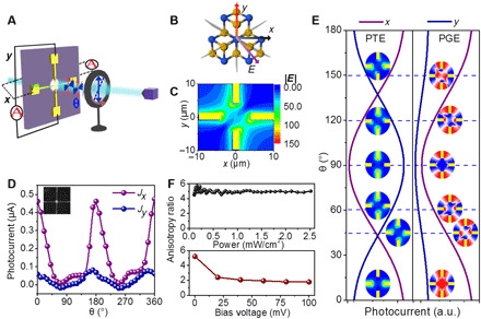
(A) Schematic diagram of the polarization-resolved photocurrent measurement setup. (B) Ideal microscopic diagram of polarization field and relative direction of material. (C) Simulated electric field distribution at specific polarization angle (45°). (D) Dependence of the photocurrents (Jx, Jy) along two orthogonal axes on the polarization angle θ (inset: scanning electron microscope image of the four-terminal PdTe2-based device). (E) Comparison of theoretical results of PGE and PTE in x and y directions. (F) Relationship between anisotropic ratio (Jx/Jy) and incident power (top) and bias (bottom).