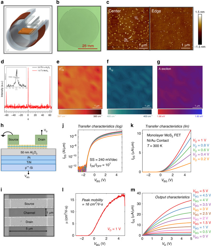
Fig. 1. Monolayer MoS2 synthesis, characterization, and device fabrication.
a Schematic of cold-wall horizontal reactor setup. b Coalesced monolayer MoS2 film grown on a 2-inch sapphire substrate using MOCVD at 1000 °C with Mo(CO)6 and H2S as precursors. c AFM images at the center and edge of the wafer showing uniform surface coverage, film morphology, and thickness. d In-plane X-ray diffraction showing the epitaxial relation between MoS2 and sapphire as (100) MoS2 ‖ (100) α-Al2O3. The inset shows a narrow full-width half-maximum (FWHM) of 0.27°, which emphasizes the high crystalline quality of these monolayer films. Raman map of (e) and (f) A1g peaks show <5% variation and the peak separation of 18 cm−1 confirms monolayer MoS2. g Photoluminescence (PL) map shows an intense peak at 1.84 eV, which is attributed to the indirect to direct bandgap transition in monolayers and is severely suppressed in multilayers of MoS2. h Schematic and i SEM image of monolayer MoS2 FET. j Logarithmic scale and k linear scale transfer characteristics of monolayer MoS2 FET measured at different drain biases (VD). l Mobility plot and m output characteristics measured at different back gate biases (VBG).

