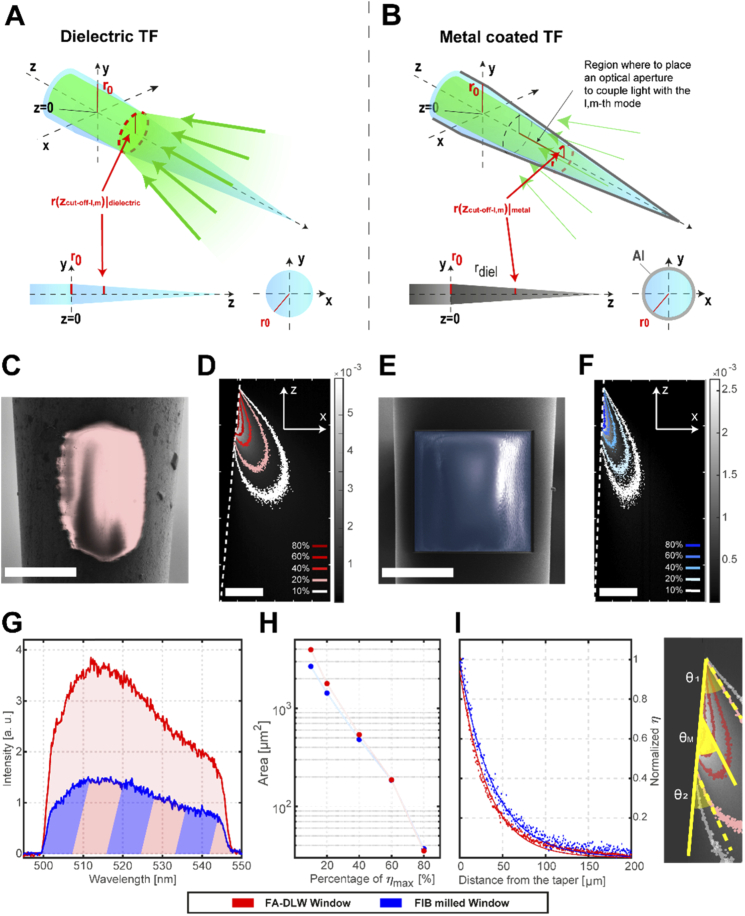
Fig. 3.
(a) Schematic representation of a dielectric TF. (b) Schematic representation of a metal coated TF. (c) Scanning Electron Micrograph of a 2PFA-DLW window. Scale bar is 25 µm. (d) Collection efficiency map for 2PFA-DLW window (red). Scale bar is 20 µm. White dashed line represents the edge of the fiber. (e) Scanning Electron Micrograph of a 40 × 40 µm2 FIB milled window. Scale bar is 25 µm. (f) Collection efficiency map for FIB milled window (blue). Scale bar is 20 µm. White dashed line represents the edge of the fiber. (g) Spectra registered for the two type of windows. (h) Collection areas at different percentages of the maximum collection efficiency value. (i) Decay profile for normalized collection efficiencies. The decay is measured along a straight line which starts from the center of the window and forms with the taper edge (white dashed lines in Figs. 3(d) and (f)) an angle equal to θM, that is the mean between the angles formed by the taper edge and the two edges of the 20% iso-surface profile (θ1 and θ2, example on a detail from Fig. 3(d)).

