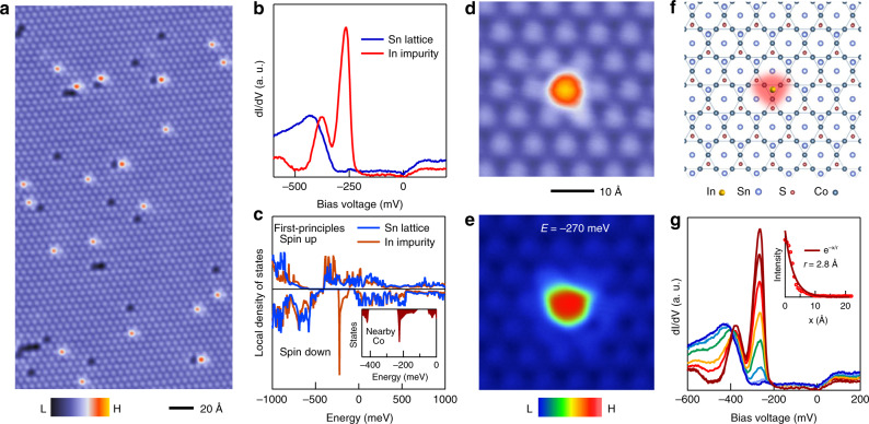
Fig. 1. Engineered atomic impurity state in a topological magnet.
a Atomically-resolved topographic image of Sn layer of 1% In doped Co3Sn2S2. b Differential conductance spectrums taken on the Sn lattice (blue) and at the In impurity (red), respectively. c First-principles calculation13 of the spin-resolved local density of states of the Sn lattice (blue) and an In impurity (red), which shows a magnetic impurity resonance. The inset shows the spin-down states of the Co atom closest to the In impurity. d Topographic image of an isolated impurity. e Corresponding differential conductance map taken at E = −270 meV (resonance energy). f Correlation between the atomic structure and the pattern in the differential conductance map. g Differential conductance spectra taken across the surface with spatial variation from the center of the In impurity (dark red) to far away (blue). The inset shows the exponential fit to the spatial decay of the impurity resonance.

