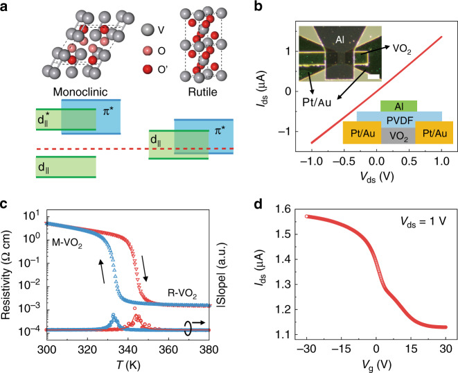
Fig. 1. Structure and electronic characterization of VO2.
a Schematic of the crystal structure and band structure of monoclinic and rutile VO2. b Output characteristics of the P(VDF-TrFE)-gated VO2 FET; the insets show the schematic and corresponding optical image. Scale bar, 20 μm. c Resistivity of the VO2 film measured under vacuum as a function of temperature (red, heating; blue, cooling). The lower points and fitted curves show the abs(slope) of the resistivity. d Transfer characteristics at Vds = 1 V of the VO2 FET.

