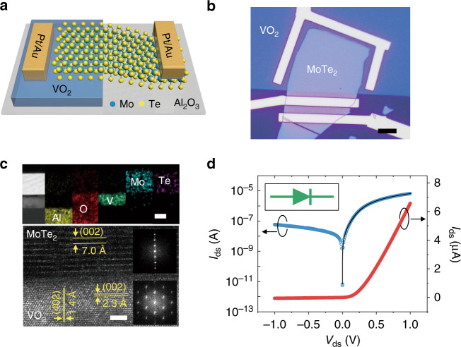
Fig. 2. Structure and properties of the heterostructure.
a, b Schematic and optical micrograph of the VO2/MoTe2 heterostructure on a sapphire substrate. Scale bar, 10 μm. c Cross-sectional TEM image and corresponding EDS mappings of the heterostructure. Scale bar, 20 nm (top); an HRTEM image of the interface of the heterostructure is shown at the bottom. The insets show the corresponding fast Fourier transform patterns indexed to MoTe2 and VO2. Scale bar, 2 nm (bottom). d Linear plots (red) and logarithmic plots (blue) of Ids as a function of Vds. The inset symbol represents the junction mode.

