
Fig. 4. Rubbery logic gates based on the freestanding composite nanofilm.
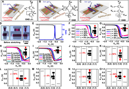
(A to C) Schematic illustration and a circuit diagram of the stretchable inverter, NAND gate, and NOR gate. (D) Photograph of the rubbery inverter, NAND gate, and NOR gate. (E) Representative VTC of the rubbery inverter. (F and G) VTC of the rubbery inverter under different strains (0, 10, 30, 50, and 0% released) along (F) and perpendicular (G) to the channel length direction. (H and I) Changes of the VTC after stretch-release cycles at 30% strain along and perpendicular to the channel length direction. (J to L) Output characteristics of the rubbery NAND gate under Vdd of 1 V under mechanical strains of 0% (J) and 50% along (K) and perpendicular (L) to the channel length direction. (M to O) Output characteristics of the rubbery NOR gate under Vdd of 1 V under mechanical strains of 0% (M) and 50% along (N) and perpendicular (O) to the channel length direction.