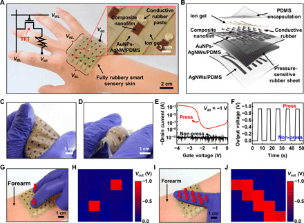
Fig. 5. Fully rubbery smart skin.

(A) The rubbery smart skin adheres and conforms to the back of the human hand. The left inset shows the circuit diagram of the smart skin. (B) Schematic illustration of the smart skin. (C) Device under stretching and twisting deformations. (D) Device under poking deformation. (E) Transfer curve with/without pressing (circuit diagram for measurement is present in fig. S23). (F) Output voltage with/without pressing (circuit diagram for measurement is fig. S24). (G) Optical image of the smart skin pressed at two points. (H) Output voltage mapping for (G). (I) Optical image of the smart skin pressed in a line. (J) Output voltage mapping for (I). Photo credit: Ying-Shi Guan, University of Houston.
