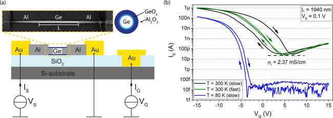
Figure 1.
(a) Schematic and SEM image of an Al–Ge–Al NW heterostructure embedded in a back-gated FET architecture. The length and diameter of the actual NW are L = 1940 nm and d = 30 nm, respectively. A cross-section of the Ge channel enwrapped in a 20 nm Al2O3-shell is schematically shown in the upper right corner. (b) Transfer characteristics of a Ge NW FET device at a bias of VS = 0.1 V recorded at T = 300 K (black and green) and T = 80 K (blue) for gate voltage sweeping rates of 0.25 and 2.5 V/s, denoted slow and fast sweeping, respectively. The arrows indicate the gate voltage sweeping direction.

