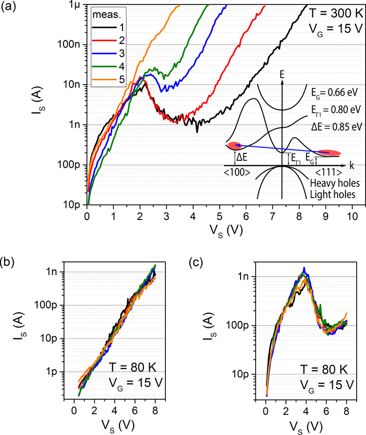
Figure 4.

I/V curves of the Ge NW device with L = 920 nm and d = 30 nm measured at VG = 15 V in intervals of 1 min. Prior to the measurements, the traps were depleted at VG = −15 V for 60 min. (a) At T = 300 K, clear indications of NDR are visible during the first 4 measurements where the predominant transport mechanism is n-type. After about 5 min, when the polarity has changed back to hole-dominated electrical transport, the NDR effect disappears completely. The inset shows the band diagram of Ge with the electric field induced electron transfer from the ⟨111⟩ valley into the ⟨100⟩ valley. The polarity can be conserved by cooling down the previously depleted Ge NW device for 60 min at VG = −15 V. (b) Upon abruptly switching the gate voltage at T = 80 K to VG = 15 V, the device remains in the hole-driven transport regime resulting in a linear I/V characteristic. (c) After the initial trap depletion procedure (VG = −15 V for 60 min), the device was cooled down to T = 150 K and the gate voltage was abruptly changed to VG = 15 V to initiate n-type behavior. A subsequent cooldown to T = 80 K conserved the electron-dominated transport.
