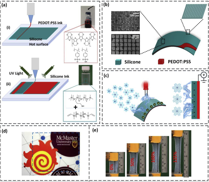
Figure 1. 3D printing process, architecture along with the optical and mechanical properties of a snow-TENG.
(a) Schematic illustration of the printing process of a snow-TENG, (a–i) printing of a conductive polymer electrode; inset shows the chemical composition of the PEDOT: PSS ink, (a-ii) Printing of the triboelectrification layer based on UV curable silicone ink; inset reveals the chemical composition of the silicone ink. (b) Schematic illustration of the structure of the device, featuring a micropatterned surface of the UV curable silicone. SEM images on the left are showing the micropattern at different magnifications. Scale bars are 100 μm and 50 μm, respectively. (c) The working principle of the device based on snow triboelectrification. (d) A photograph showing the high transparency of the silicone layer; the logo of McMaster University shown in the background can be recognized through the silicone layer. (e) Exposure of the snow-TENG to different stretching conditions.

