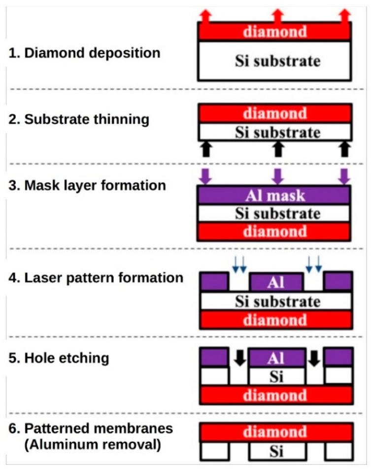
Figure 1.
Scheme for the polycrystalline diamond membranes fabrication: (1) CVD growth of PCD films on Si substrate; (2) Thinning of the Si substrate with inductively coupled plasma etching; (3) Deposition of the thin aluminum mask; (4) Formation of windows in the Al mask using the excimer laser; (5) Local etching of Si substrate with the inductively coupled plasma etching technique; (6) Removal of the residual Al layer.

