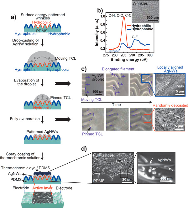
Figure 2.

a) Scheme describing the fabrication process comprising chemical and physical modification of the PDMS substrate, deposition and alignment of AgNWs, and coating of the thermochromic layer. b) XPS analysis of partially patterned surface of wrinkled PDMS substrate. Inset: optical microscopy (OM) image of the PDMS wrinkles. c) Sequential OM images of an AgNW‐containing evaporating droplet on the hydrophobic and hydrophilic wrinkled surface. Insets are SEM images of the evaporation‐induced AgNW morphologies (locally aligned and randomly deposited AgNWs) on a PDMS wrinkled substrate with patterned surface energy. d) Cross‐sectional SEM images of the integrated device.
