Figure 2.
Electronic Performance of Flexible In2O3 Nanoribbon Field-Effect Transistors
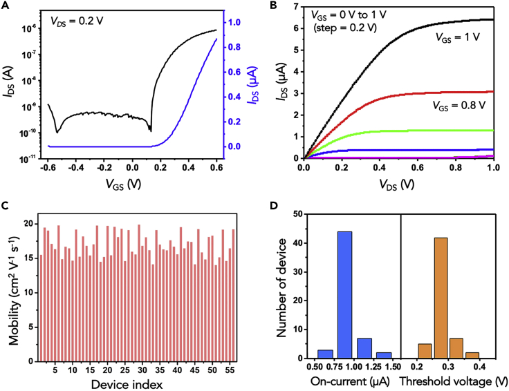
(A) Representative transfer characteristics of an In2O3 nanoribbon transistor with L = 500 μm, W = 25 μm, and H = 16 μm in phosphate buffered saline. The ID (drain current) is shown in a logarithmic scale (left, black trace) and a linear scale (right, blue trace); VGS is the gate-source voltage. The applied drain-source voltage VDS was 0.2 V.
(B) Output curves in the linear and saturation regimes. In this plot, IDS is a function of VDS with VGS from 0 to 1 V in 0.2-V steps.
(C) Plot of the charge-carrier mobilities of 56 transistors in an array.
(D) Histograms showing on-currents and threshold voltages from the same 56 transistors. The average mobility was 17.8 ± 1.8 cm2 V−1 s−1. The average on-current was 0.86 ± 0.1 μA. The average threshold voltage was 0.27 ± 0.02 V.
See also Figure S2.

