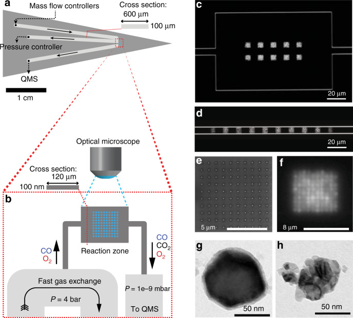
Fig. 1. Reactor chip layout and optical readout.
a Schematic of the micro- and nanofabricated reactor chip comprising a microfluidic in- and outlet system that connects to the model catalyst bed, as well as the high-pressure gas handling system and the QMS, respectively. The cross-sectional dimensions of the microfluidic channels are also shown. Arrows indicate flow direction. b Schematic depiction of the model catalyst bed (reaction zone) of the chip that contains the catalyst nanoparticles and the corresponding cross-sectional dimensions of the well-mixed reactor in (c). Note that the schematics are not drawn to scale. The entire catalyst bed is imaged by dark-field optical microscopy that resolves all particles individually based on their optical scattering signature. c Dark-field scattering image of a well-mixed catalyst bed with dimensions 180 μm × 120 μm × 100 nm (L × W × H), containing ten Cu nanoparticle array patches, each comprising 100 individual particles with a diameter of 120 nm and a thickness of 40 nm. d Dark-field scattering image of the plug-flow catalyst bed consisting of a straight channel with 10 μm × 100 nm cross section and decorated with ten array patches, each comprising 100 individual particles with the same dimensions as in (c). e SEM image of a 100 Cu nanoparticle array patch. f Zoom in dark-field image of a 100 Cu nanoparticle array patch. g TEM image of a representative single Cu nanoparticle reduced in 1.2% H2 at 400 °C. The slight surface oxide stems from exposure to air during transport to the TEM. h TEM image of a representative Cu nanoparticle oxidized in 0.2% O2 at 400 °C, revealing the dramatic structural changes oxidation can induce.

