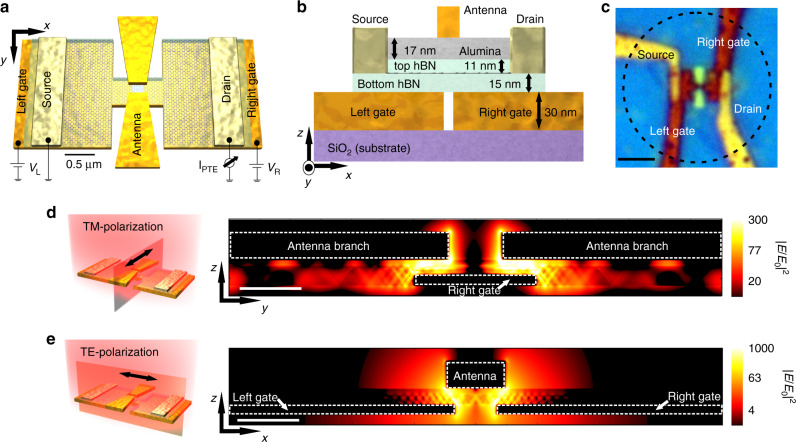
Fig. 1. Device schematic and operation principle.
a Schematic representation of the photodetector consisting of H-shaped resonant gates of 4.2 μm of total length, with a hBN-encapsulated H-shaped graphene channel transferred on top, contacted by source and drain electrodes. A bow-tie antenna of 2.7 μm of total length is placed on top of the 2D stack. The local gates serve to create a pn-junction in the central part of the graphene channel (by applying voltages VL and VR), where the antenna gap and gate gap are located. Both narrow gaps are on the order of ~100 nm. The scale bar corresponds to 0.5 μm. b Side view of the device design (not to scale) with indications of the materials' thicknesses. c Optical image of the photodetector. The dashed lined circle indicates the typical beam spot size obtained at λ = 6.6 μm. The scale bar corresponds to 2.5 μm. d Cross section view of the simulated total electric field intensity (∣E∣2) normalized to the incident one (∣E0∣2) along the antenna main axis when light is polarized parallel to the bow-tie antenna (TM-polarization) axis as indicated in the illustration on the left. The white scale bar corresponds to 250 nm. e Same as (d) but for light polarization perpendicular to the bow-tie antenna (TE-polarization) and parallel to the local gates as shown in the schematic on the left.

