Figure 4.

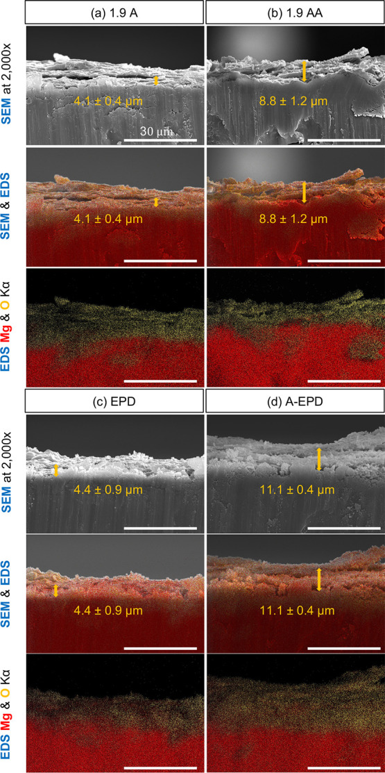
Cross-sectional characterization of the surface-treated Mg samples by SEM and EDS. Montage of SEM images, and overlaid images of SEM and EDS maps of O (yellow), Mg (red), and K (blue), as well as the corresponding overlaid EDS maps (Kα line) for the elemental distribution of O and Mg. (a) Anodized Mg (1.9 A); (b) annealed-anodized Mg (1.9 AA); (c) Mg with electrophoretically deposited MgO nanoparticles (EPD); and (d) Mg with electrophoretically deposited MgO nanoparticles and annealed (A-EPD). SEM images were obtained at an original magnification of 2000×. Scale bar = 30 μm for all SEM images and EDS maps. The average thickness of the oxide layers on Mg substrates was labeled in the SEM images, and overlaid images of SEM and EDS maps of O (yellow), Mg (red), and K (blue), as denoted using the double sided arrows and values of mean ± standard deviation (SD).
