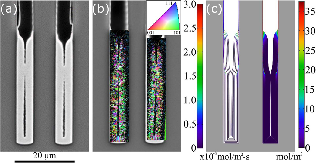
Figure 9.
a) Scanning electron microscope image of a cross-sectioned annular TSV after Ni deposition in electrolyte containing 10 μmol/L PEI for 20 min at −1.23 V then 20 min at −1.27 V. The image is from the same specimen as Fig. 8 but has been cropped to focus on the Ni deposit. b) The microstructure of the TSV characterized using electron backscatter diffraction. The texture map corresponds to the grain orientation normal to the TSV sidewalls. Dark regions indicating decreased grain size or degraded crystallinity are visible at the top of the metal deposit and adjacent to the deposit bridging the central void. Tilt of the void in the lower region and misaligned scan area in the righthand map result from beam drift during the scan. c) Simulation of additive incorporation in the Ni deposit for the experimental growth conditions, with other parameters from Table I. The left side shows the rate of PEI incorporation (Eq. 3, Γk_vθ) on growth contours at 5 min intervals; the right side shows a map of the resulting PEI concentration in the deposit. The color scale saturates at roughly half the maximum predicted value, found only in the passive deposits lining the upper sidewalls. The regions of elevated PEI incorporation exhibit reduced grain size in the EBSD map. The diagonal white lines emanating from the bottom corners are artifacts of plotting.

