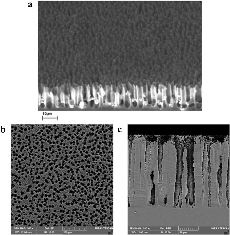
Fig. 2.
(a) SEM micrograph of a typical PtSi/Porous Si sample. The white areas at the walls of the pores are PtSi. As it can be seen, the pore openings are a few μm wide and their depth is about 10 μm. The porosity at the scale of the device is uniform and reproducible as witnessed in reproducible IV characteristics. Liquid enters the pores and makes contact with the PtSi covering the sidewalls. The PtSi layer creates the bright white areas seen in the graph. (b) The porous samples of which results are provided in this paper. Porosity is such that pores with a diameter of 10 μm are surrounding pores similarly to Fig. 1a. (c) The depth of the large pores reach down to 70 μm. This porosity has been used to help liquids with higher surface tension to enter the pores as well.

