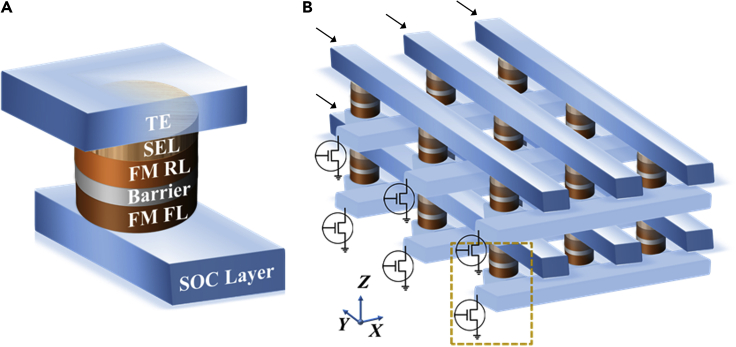
Figure 4.
A Proposed 3D SOT-MRAM
Schematic of proposed single two-terminal SOT-MTJ cell (A) and the corresponding integrated 3D SOT-MRAM architecture (B). Writing and reading currents can be addressed to a specific MTJ cell by controlling the transistor switches and selectors. FL, free layer; RL, reference layer; SEL, selector; TE, top electrode.

