Figure 2.
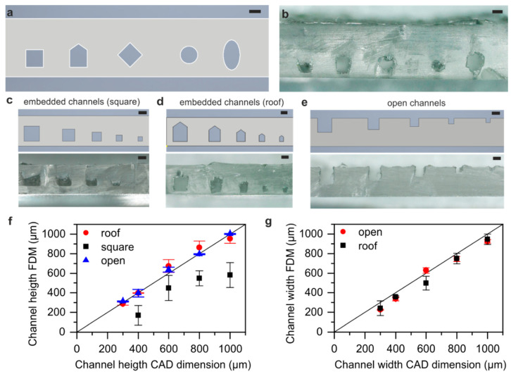
Characterization of the channel cross-section of a printed PMMA chip. (a) Image of the design of the printed channel cross-sections. (b) Different channel cross-sections with a channel width/diameter of 600 µm printed in PMMA. (c) Fused deposition modeling (FDM) printed embedded channels with a square cross-section for analysis of the printed channel height. Due to sagging the channel height deviates strongly from the original CAD design. (d) FDM printed embedded channels with a roof shaped cross-section for analysis of printed channel height and width. The addition of the roof compensates the sagging resulting in square channels. (e) Open square cross-section channels for analysis of the channel height and width. (f) Comparison of channel heights of embedded FDM printed channels using square and roof shaped cross-sections shown in (c,d) and open channels shown in (e) with the designed CAD heights. (g) Channel width of open and embedded roof shaped FDM printed channels from (d,e) compared to the designed CAD widths. (Scale bars (a–e): 500 µm).

