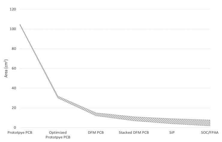
Figure 7.
Board/Package Area Projection with Different Levels of Design Integration, starting from the current prototype with the PCB size of 104 cm, followed by an optimised PCB with a 20% components density and a design for manufacturability (DFM) design with a 50% components density; further minimisation could be performed by a stacked PCB or SiP (system in package) design, or by the chip-level FPAA/SoC design.

