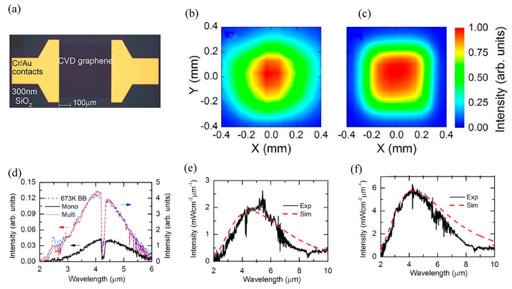
Figure 3.
(a) The device fabricated with large area graphene 0.5 × 0.6 mm, transferred on 300 nm SiO2 substrate, with CR/Ar source and drain contacts. (b,c) shows the thermal emission from single and multi-layered graphene, (b) emission from single-layer graphene with peak current injection of 44 mA, (c) emission from multi-layer graphene with peak current injection of 52 mA. (d) The emission spectra of single and multi-layered graphene, calibrated with the back body at 673 K, where the peak emission was approximately 4 um and the large deep trench at 4.2 µm was ascribed to the CO2 absorption. (e,f) shows the measured and simulated spectra with a dash [61].

