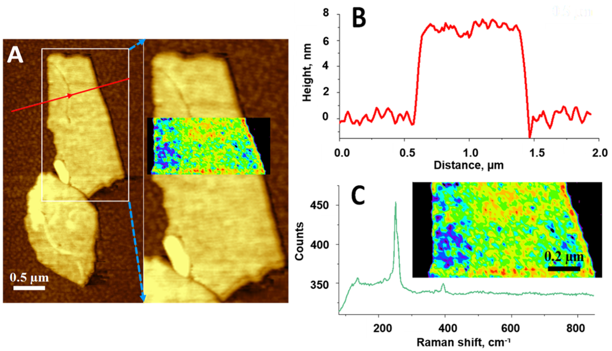
Figure 1.

(A) Topographic AFM image of WSe2 flakes on an Au-on-Si substrate. The measured height of these flakes is about 7 nm and is uniform across the sheets, as illustrated by a cross-sectional height profile in panel B. Panel A also shows a 1.2 μm × 0.6 μm TERS image (88 pixels/line, 13.6 nm/pixel) where the intensity of the peaks within the 235–270 cm−1 range is overlaid over the topographic AFM image. The TERS image is expanded in the inset of panel C, which also shows the spatially averaged TERS spectra of WSe2 that exhibit the familiar resonant Raman response of this system following red-laser excitation. Rather sharp edges of the flake are evident in the TERS map, which is indicative of strong TERS enhancement and nearly pixel-limited spatial resolution.
