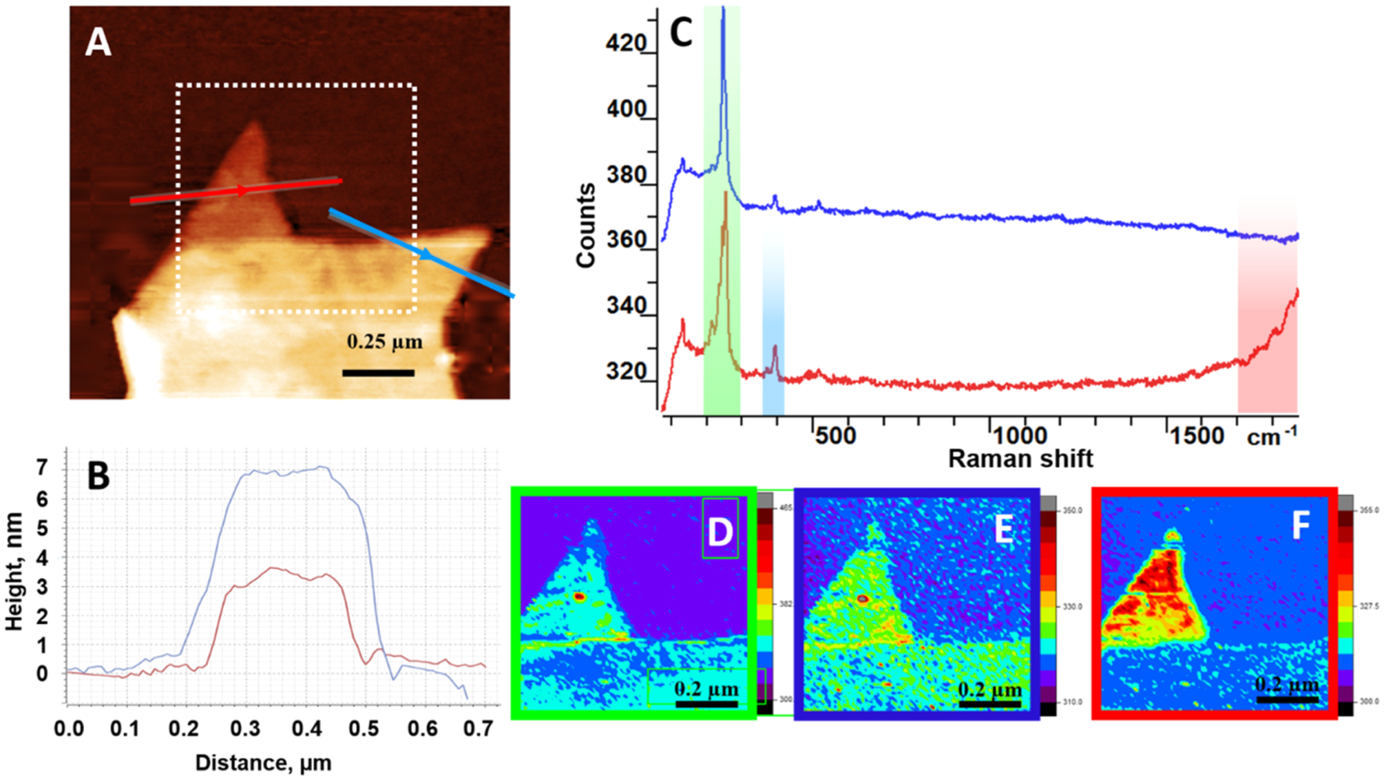
Figure 4.

(A) Topographic AFM image of the WSe2 flake on Cr surface. (B) Corresponding profiles along the red and blue lines in panel A, featuring two distinct parts of the flake with approximate heights of 3 and 7 nm, respectively. (C) TERS/TEPL spectra from the 3 nm (red line) and 7 nm (blue line) thick areas, offset vertically by 50 counts for clarity. TERS (Panels D, E) and TEPL (panel F) maps from the square area, indicated by a dotted square in panel A. The spectral window for each map is: (D) from 195 to 295 cm−1 (green band in panel C), (E) from 360 to 420 cm−1 (blue band in panel C), (F) from 1700 to 1850 cm−1 (red band in panel C).
