
Figure 1. Fundamental Working Principles of the Hierarchical Loading Microwell Chip.
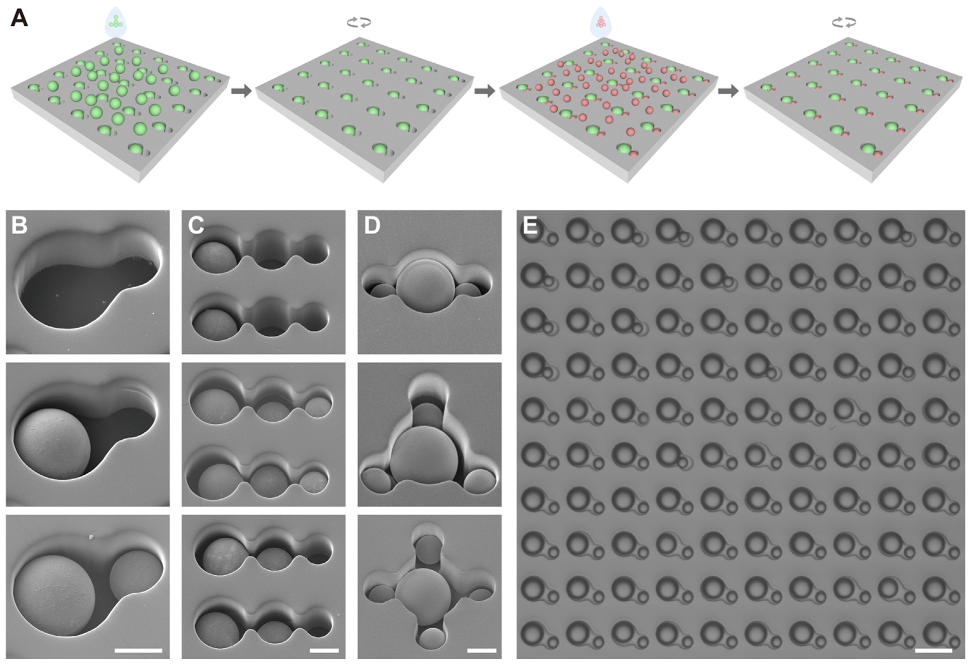
(A) Schematic loading processes of a dual-well HL-Chip.
(B) Representative scanning electron microscope (SEM) images of a dual-well HL-Chip unit with graded loading of beads.
(C) Representative SEM images of tri-well HL-Chip units with graded loading of beads.
(D) Representative SEM images of large well-centered HL-Chip units loaded with beads.
(E) A representative microscopic image of a block of a dual-well HL-Chip loaded with beads.
Scale bars for (B)–(D) are 10 and 30 mm for (E). See also Figure S1.