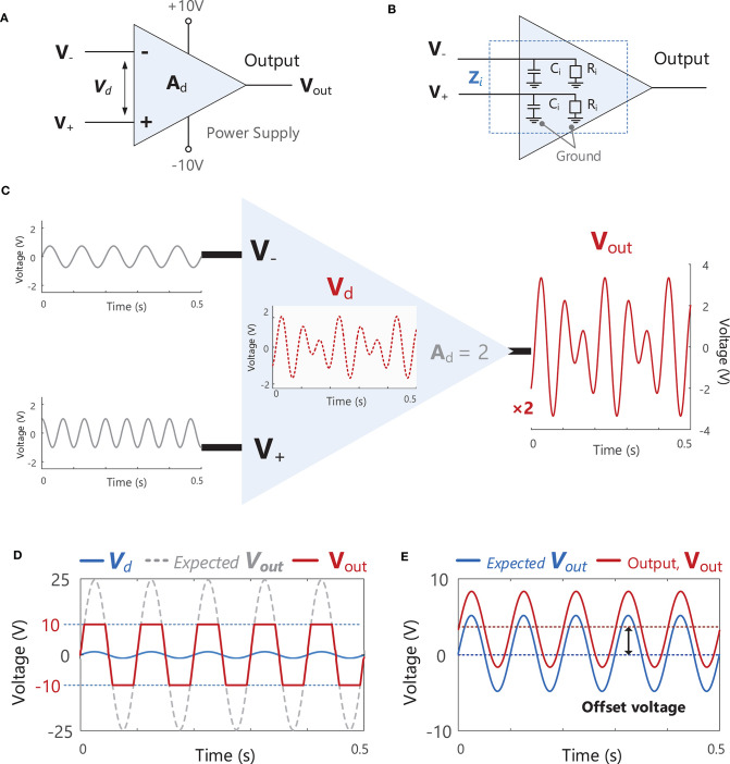
Figure 7.
(A) A schematic of an ideal differential amplifier with two inputs V− and V+, an output Vout and power supply connections (+10 and −10 V). (B) A schematic of the internal input impedance, Zi. present at both amplifier inputs V− and V+. Zi consists of a resistive component, Ri, and a capacitive component, Ci. (C) A schematic illustration the function of a differential amplifier, which receives two input signals at V− and V+, calculates the difference between these signals, Vd (Vd = V+ - V−), and multiplies (amplifies) Vd by the gain of the amplifier, Ad (in this example the signal is increased by a factor of 2). See Example (xii) in Tutorial Code. (D) If the gain of the amplifier is increased to a level where the expected Vout exceeds the level of the power supply voltage (e.g., ± 10 V in the amplifier shown in A), the actual Vout will be “clipped” or “limited” at the power supply voltage. (E) An example of an offset voltage being present in the amplifier output, Vout.

