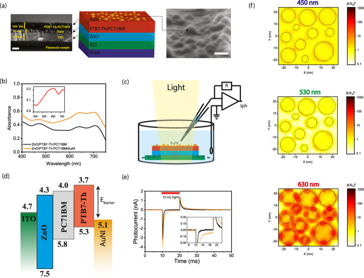
Figure 1.
(a) (Left) Cross-sectional scanning electron microscopy (SEM) image of the plasmonic biointerface (scale bar, 100 nm). (Middle) Schematic device structure of the plasmonic (ITO/ZnO/PTB7-Th:PC71BM/AuNI) biointerface. (Right) SEM image of nanoislands at the plasmonic biointerface (scale bar, 20 nm). (b) Absorption spectrum of ZnO/PTB7-Th:PC71BM (black line) and ZnO/PTB7-Th:PC71BM/AuNI (orange line) thin films. The inset shows absorbance of the AuNI layer (red line), which is calculated by extracting it from the control biointerface without the gold layer that has a smooth surface due to the absence of nanoislands (Figure S1a,b). (c) Schematic of the photocurrent measurement setup. The patch pipette is kept close to the surface, and the current is measured with a voltage-clamp mode. (d) Energy band diagram of the plasmonic biointerface (with respect to vacuum). (e) Photocurrent of control (black line) and plasmonic (orange dotted line) biointerfaces illuminated under green light at 8.8 ± 0.2 × 10¹⁶ photons s–1·cm–2 with 10 ms pulse widths. The inset zooms on low photocurrent levels. The capacitive current amplitude is defined as the maximal current amplitude reached after the light onset. The faradic current is defined as the current amplitude for 9 ms after the start of illumination (Figure S5). (f) Lumerical FDTD simulation of AuNI of the plasmonic biointerface. Top, middle, and bottom panels show field profiles at 450, 530, and 630 nm, respectively. KEelectron = Ephoton – Ebarrier – Edeep traps, Ebarrier = 1.4 eV, Edeep trap = [0.5–0.8] eV. KEelectron at 450 nm = 2.75–1.4–0.8 = +0.55 eV, KEelectron at 530 nm = +0.14 eV and KEelectron at 630 nm = −0.23 eV. While there is hot-electron injection in blue and green spectral regions, we observe the nanoantenna effect at the red spectral region.

