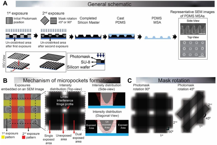
Figure 1.
Fabrication of DEL-MSAs (dual-exposure lithography-microstructure arrays). (A) General schematic of microstructure array (MSA) fabrication through dual-exposure lithography (DEL). The SU-8 photoresist was exposed twice using a strip-patterned film mask. The initial position of the film mask was at 0° and re-oriented to 45° or 90° (in the xy-plane, along the z-axis) between exposures. The crosslinking energy of two exposures overlapped with each other, creating tapered overcut 3D micro-pockets. Soft lithography was used to mold DEL-MSAs in polydimethylsiloxane (PDMS). (B) Mechanism of micro-pocket formation. Left: Patterns of two exposures overlaid on an SEM image, along with an illustration of the intensity distribution from exposed areas to unexposed ones (on x-y axis). Black lines in the unexposed area illustrate the interference fringe pattern. Right: A side view and a diagonal view of the intensity distribution profile (on the z-axis). Red lines indicate the anisotropic intensity distribution in the unexposed areas. The aspect ratio of the micro-pockets was tuned by tuning the fabrication parameters (exposure energy, angle of rotation, and wait time between exposures). (C) Top-view schematic of mask rotation effect on the intensity distribution, forming different borders of microstructure. Black arrows denote the rotation angle between first and second exposure. Scale bar: (A) 100 μm; (B) 10 μm.

